Atmospheric: a dual-sensor board featuring an STM32 MCU and SD card read and write functionality. In this post, I will go into detail regarding the process of schematic creation, as well as Printed Circuit Board (PCB) layout and routing.
Schematic Design
Schematic design is an integral part of electrical engineering. Schematics are the colloquial map of a board, allowing you to design, assemble, and fix issues. This process always starts with component integration, which I mentioned in the previous post. The first step is to find the datasheet of the component to be integrated and then the footprint information. This is because I generate most components’ footprints with the built-in IPC footprint wizard in Altium Designer. This fantastic tool also creates 3D models of each of the components I integrate – unless the component involves an uncommon package. In this case, I manually make the footprint and sometimes make the 3D file using CAD software.
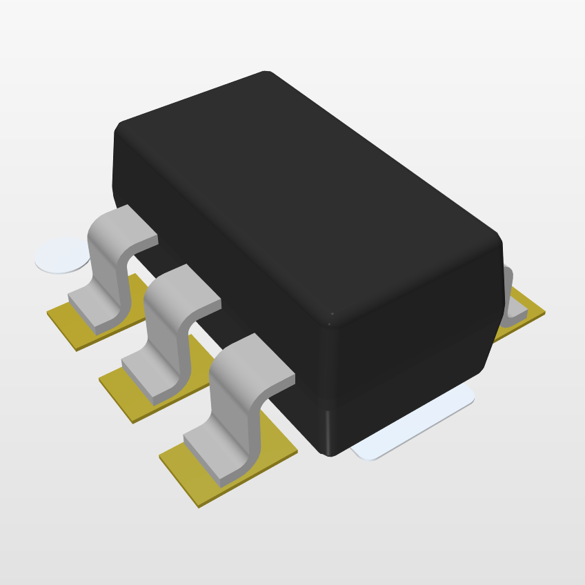 An auto-generated 3D footprint of a SOT23 component package
Once the components have been integrated, schematic design starts to take place. Components are laid out into their own areas designated by function. For example, a battery charger IC will be placed with its decoupling capacitors and tuning resistors in the same part of the schematic to reduce clutter. This can be seen in the image below, which shows a large portion of the schematic for the board.
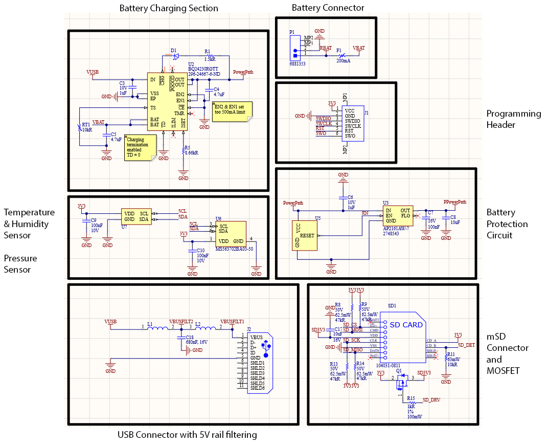
After the individual “sections” of the schematic were completed, I connected them based on their purpose. For example, I connected the sensors to the microcontroller over the I²C communication protocol so that they could communicate (bi-directionally!).
Schematic Verification
In schematic verification, I go over the fundamental aspects of the board and make sure that they are functioning correctly. For example, I also checked that the core power rails (3V3 and GND) are connected to each component, with their respective capacitors. Furthermore, the power from the battery goes through several components, which is why I made sure to thoroughly check that they were set up correctly. There is no particular method I use for schematic verification. Instead, I tend to look at the individual components’ datasheets to make sure my implementation of their function is in accordance with their spec. This will include me going over the typical application schematic that is generally found in most component datasheets.
PCB layout
Once I (roughly) verified the schematic of Atmospheric, I started with the first step of the PCB routing: component layout. I wanted to keep the sensors on the side of the board to reduce the thermal inertia. The general rules also applied when doing the layout, such as placing decoupling capacitors as close as possible to the IC they’re filtering. The reason for this is something I will get into in a future blog. Still, in short, it acts as a minuscule battery, providing instantaneous current and preventing noise in the power rails. This noise could affect other ICs using the same power rail, so it is essential to minimise all noise where possible. There are also general “rules” for PCB layout, but I feel like you will fall asleep if I list them.
Once the components were placed logically (based on their function) and I felt there weren’t unnecessary amounts of space, I started the PCB routing.
PCB routing
PCB routing, in my opinion, is the most fun part of the whole circuit design process. It can also be the most irritating. Routing is the process of joining together points on the circuit board with traces or planes, following the schematic and design rules. Traces are just like wires, but they’re embedded on a circuit board. The general idea of PCB routing to never use the auto-router. Only joking! The first actual requirement is probably to figure out what the capabilities of your PCB fabrication company are. For example, the Atmospheric board was fabricated by Oshpark and the stencils from Oshstencils. Once I had figured out what the capabilities of Oshpark were, I set up the design rules. This allowed me to check for discrepancies between the board and the capabilities of the manufacturer with the Design Rule Check tool in Altium.
Then I started routing the board. I normally try to do the power rails first, as they are usually the widest traces. This is to allow them to carry more current. Some power rails on the board were also given planes (also known as copper pours), which are usually for allowing for higher current capacity. In this project, however, it was more to reduce a phenomenon called parasitic inductance. This is another topic I will go into one day on the blog.
Once these power planes and traces were laid out, preferably with as little cross-over between the top and bottom board layer, I started the signal routing. Signal traces can be ridiculously small, with some reaching a width of nearly 0.15 mm. Some PCB fab houses even allow for traces less than 0.1 mm in width, which is insane. You could make power traces that small; it all depends on the amount of current you want to shove through them.
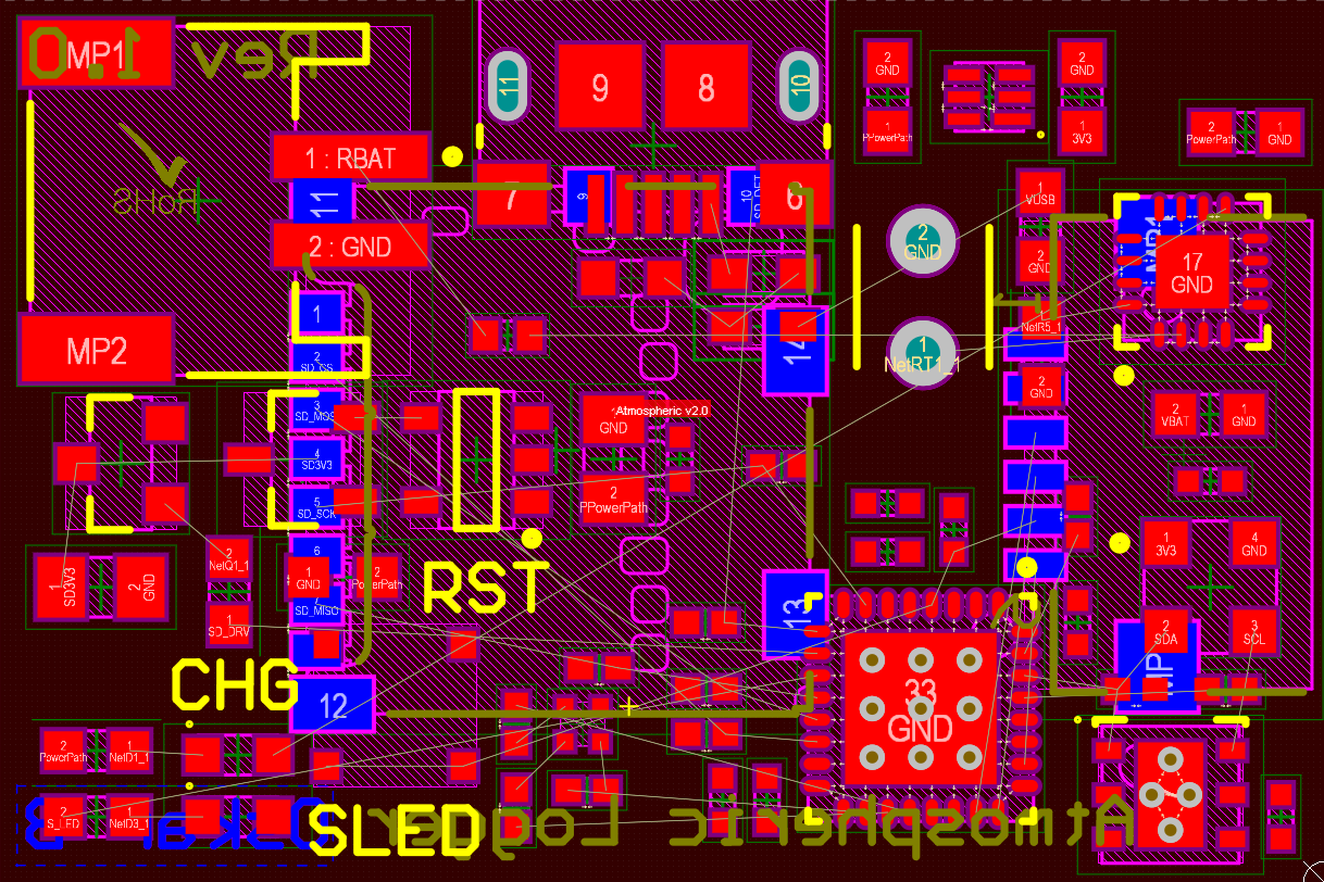
Once the signal traces were laid out like the power ones, I made sure that none were longer than they needed to be. This is because long traces increase the risk of electromagnetic interference, which is where the traces can act as receiving or transmitting antennae. This isn’t so much of an issue in Atmospheric, as it is not a high-speed circuit. However, it is still good practise to be vigilant. The final result, after fixing multiple issues presented by the Design Rule Check (such as forgetfully leaving some traces unrouted). The end result looked like this:
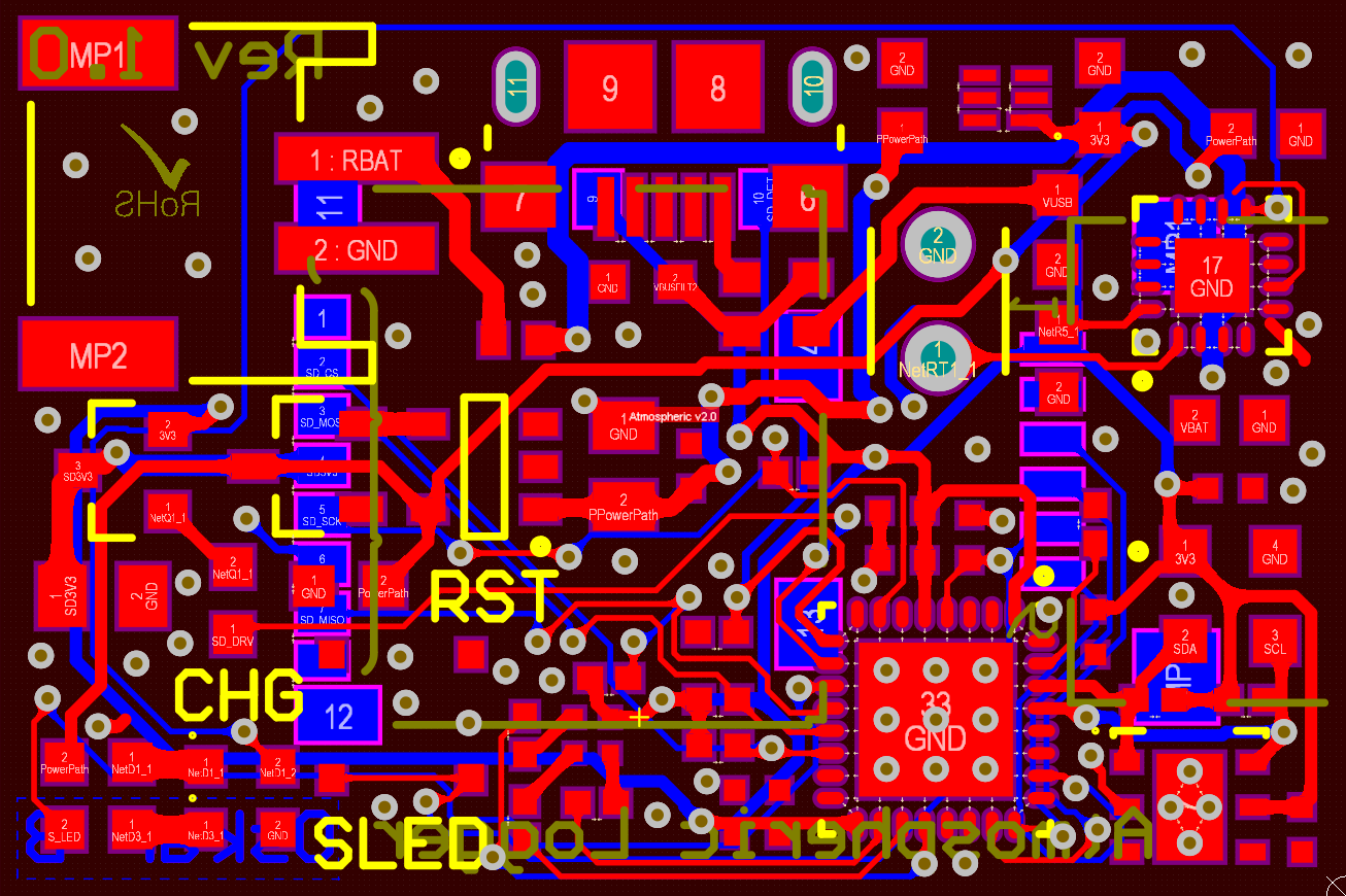
And with the polygon planes:
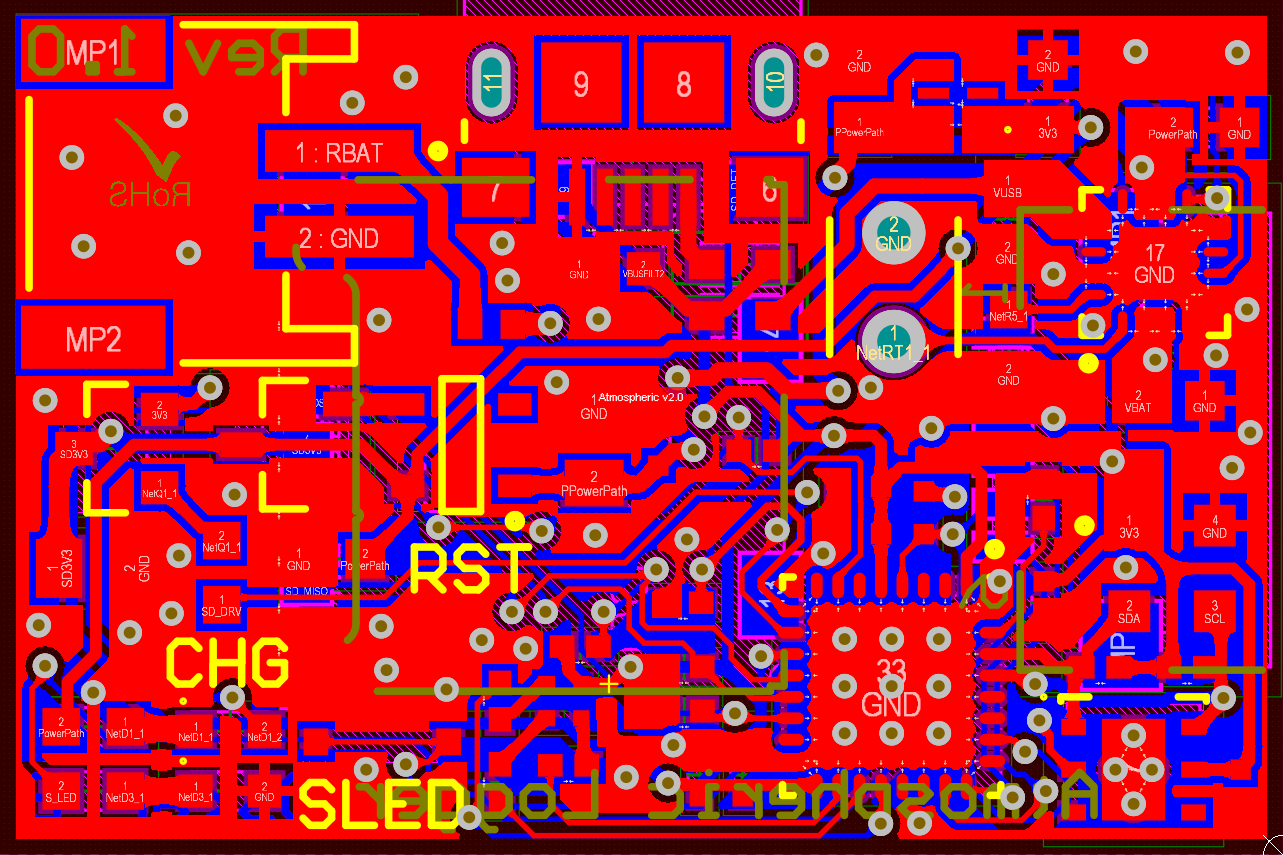
You see a colossal sea of red because, once all the traces have been routed, I placed a ground power plane on both sides of the board from edge to edge. This is really important as it can help against numerous issues, such as electromagnetic interference and ground loops.
In part III of the blog, I will discuss in more detail DRC checks, PDN analysis, BOM creation, and Gerber output for manufacturing.