Atmospheric: a dual-sensor board featuring an STM32 MCU and SD card read and write functionality. In this post, I will go into detail regarding the process of PCB verification and testing with the DRC & PDN tool. I’ll also talk about how I exported the Bill of Materials (BOM) for purchasing the components used for the board, and the Gerber files for having the PCB manufactured.
PCB Verification
Fortunately for my sanity, PCB verification isn’t as manual as schematic verification. Although others may feel it’s the other way round, I think it depends on the software. The first part of PCB verification that I undertake is Design rule checking (DRC). This is an essential part of the verification process because it points out critical issues, such as unrouted nets, shorted traces, and dimensional problems such as trace widths, via sizes, etc.
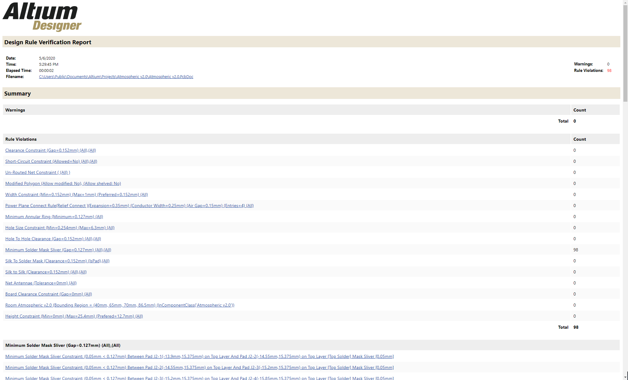
Here you can see the output of Altium’s DRC tool, which looks fantastic!
You can clearly see there is an issue (well, 98 occurrences of an issue) shown by the output of the DRC, in this case “Minimum Solder Mask Sliver”. Fortunately, this is much easier to fix than the other issues that a DRC may present. At the top of the DRC report, you can see the most critical constraint violations, such as Short-Circuits, Clearance, and Un-Routed Nets. These are the ones that I make sure to look out for the most – if you send off your board for manufacturing with an unrouted net you will be in for some sadness! When designing Atmospheric, I got my fair share of unrouted net complaints. These were all easily fixable. I luckily do not face the issue of a short circuit or clearance constraint issue that often, as Altium will normally highlight it in the PCB editor as it presents itself.
PDN Analysis
After fixing up all the issues presented by the DRC, I went on to use a tool that I had only recently acquired: the Power Delivery Network (PDN) Analyzer. This tool is an optional add-on to Altium and it’s incredible. It can clearly display to you simulated voltage and current densities across traces on your board for Power Rails. The voltage density is calculated based on the resistance of the traces, the resistance of components in series with the rail, and the current draw of components in parallel with the rail. This allows for me to figure out if the voltage at the power pins of an Integrated Circuit (IC) is sufficient, amongst other things. For example, the diagram for the battery (or VBAT) power rail for Atmospheric was set up as shown below, with the protection circuitry elements in series and their resistances noted. This allows for the voltage drop between the components to be calculated.
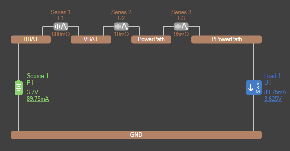
Here you can see the built-in current limiting polyfuse (F1), Battery Charger (U2), and Protection Load Switch (U3). Their individual effects on the voltage of the battery are calculated and shown. This resulted in the following diagrams:
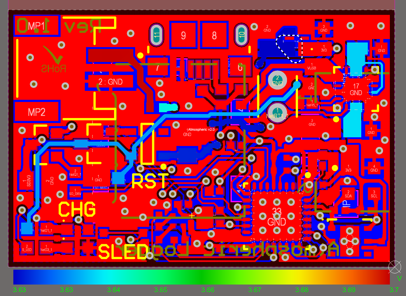
In this picture, you can see the voltage of the battery (overlayed on the relevant traces) as it passes through the protection fuse and two ICs. The voltage drop is calculated by the PDN analyser to be around 0.07 V, which is not bad! This is assuming the battery voltage is 3.7 V.
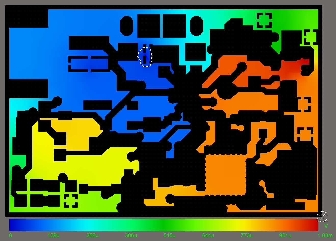
This picture shows the voltage on the ground plane, overlayed onto itself. The general idea is to try and get all of the ground planes and traces to the same potential, avoiding ground loops. Here, the voltage difference between the lowest voltage part of the plane and the highest is around 1.03 mV, which I don’t think is too bad. I say this because a difference of 1.03 mV in potential is very small. Maybe it wouldn’t be ideal for sensitive devices, but the board doesn’t qualify as such.
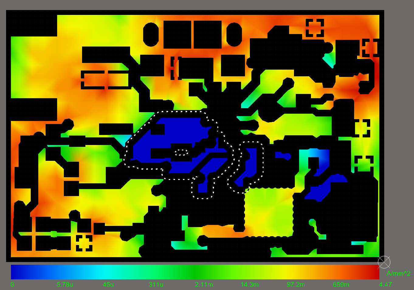
This picture shows the current density (per mm2) overlayed onto the ground plane, clearly showing where the most and least current on the board is being drawn (highlighted with the dotted line by the software). This is exceptionally useful as it allows you to decide if your traces are wide enough in certain parts of the board.
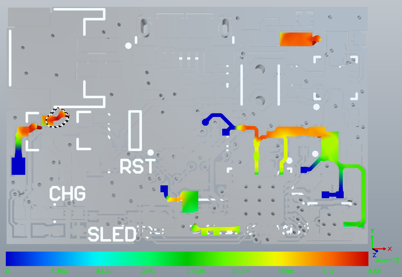
Lastly, I thought I’d add this picture as it just looks cool! Here it is overlaying the current density of the 3.3 V rail onto the 3D perspective of the board.
I didn’t just use the PDN tool just for the coolness factor, it actually helped me spot an issue: one trace wasn’t even connected properly. This naughty trace had evaded the eyes of the DRC, but clearly showed up with a voltage of 0 V when I was looking at the PDN results. This confused me, until I looked closer and realised it wasn’t connected. I don’t remember what specific power trace was unconnected, but I think it was one of the sensors’. Thus, it could have presented a disastrous issue if it had snuck its way into the manufacturing stage without me noticing. It could have potentially left one of the sensors starved for power!
After thoroughly rechecking the PCB (twice!) I exported the BOM and Gerber files. The BOM allowed me to order all the components quite easily. However, depending on your supplier of components, your mileage may vary. I’ve found Digikey and Farnell to be the best when importing a BOM. The output BOM for the atmospheric board is shown partly in the image below:
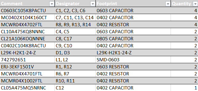
It really isn’t too exciting, so I’ll spare you the boredom of talking about it any more.
Gerber files
The last step was to export the Gerber files. This process, like the previous, isn’t as fun as the earlier steps of routing and PDN analysis. However, it has to be done to grasp your beloved board in your hand. There isn’t really much detail I can go into about Gerber file exporting because I know very little about it, just the minimum to get my boards manufactured 😊. The Gerber Files are exported in the Gerber X2 format and the NC drill files are generated to accompany them. These NC drill files are primarily used by CNC machines to mill out the holes of the PCB, such as via holes, openings for connectors, etc. Once this was done for the board, I bundled the files into a folder and sent them off to the PCB fabrication house, which was Oshpark. I also ordered stencils (from Oshstencils) to make it possible to apply the solder paste to the board accurately, as doing it blindly would have had some peculiar and upsetting results.
In the next part of the blog, I will discuss the assembly process of the board using my reflow oven!