Atmospheric: a dual-sensor board featuring an STM32 MCU and SD card read and write functionality. In this post, I will go into detail regarding the lengthy process of assembling the board (painful, I know).
Assembly
Once I had received the components and board in the mail, I started the scary process of assembly. I feel that it’s scary because this is really the only step where I can lose my money, for example if the soldering goes terribly wrong. Because of this, it can be stressful in the moment. However, I normally look forward to the assembly process because, after you are done, you (typically) have a functioning board.
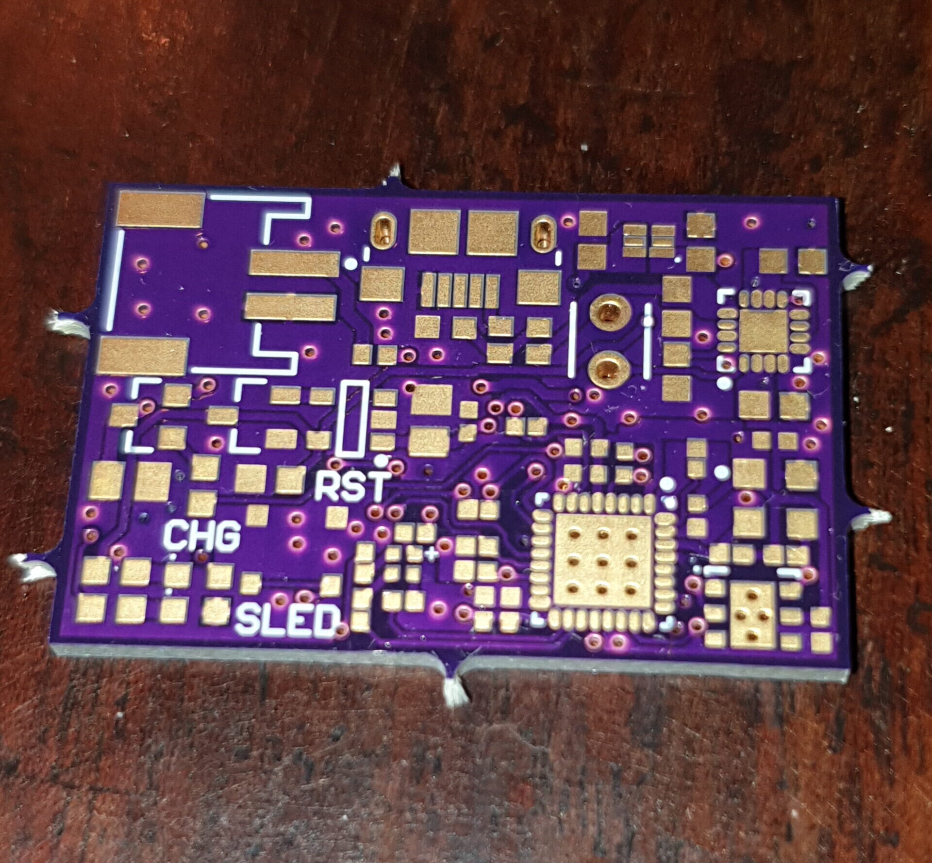
As you can see in the picture, the board from Oshpark is Electroless Nickel Immersion Gold (ENIG) plated, which is what gives the board its beautiful gold shine (literally) on the pads. ENIG is a lead-free plating method for PCBs (sorry, lead, not many people like you).
The first part of the assembly process is positioning the stencil over the board. The stencil was made from laser-etched Kapton material, which made it flexible. Because of this, I had to make sure that it was adequately taped down and aligned over the board, with no areas of flex – which would create a gap and allow for solder paste to seep in.
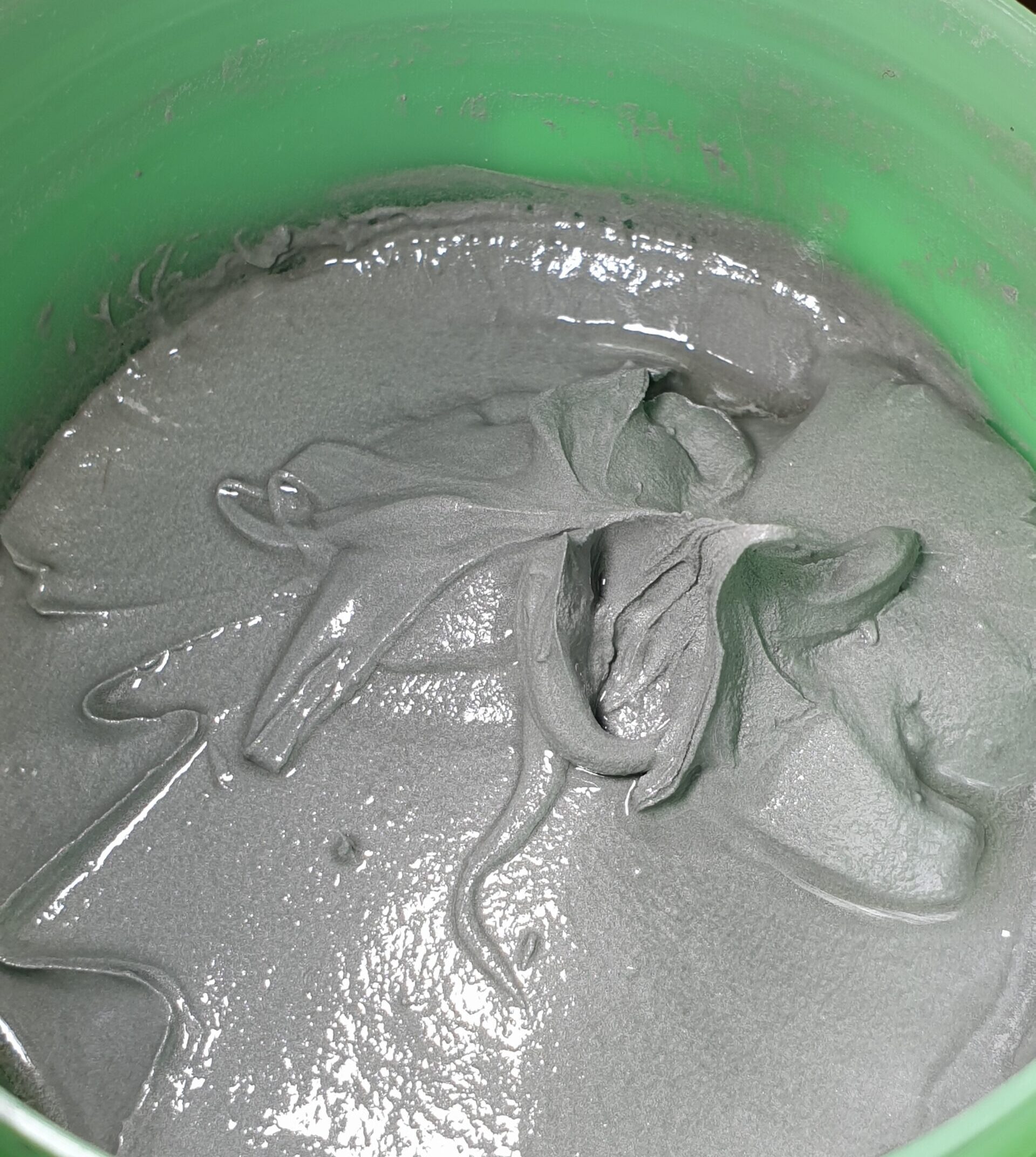
Solder paste, unlike traditional solder wire, is a paste, as its name would imply. When heated up by a hot air gun or reflow oven, the little solder paste balls (sometimes 0.015mm in diameter!) held in suspension by flux join together, and the flux evaporates. The solder paste I use is Loctite GC-10, which is remarkable. There are a plethora of reasons for this, such as the fact that it does not need to be stored in a cold environment (unlike nearly all other solder pastes) and it is lead-free. Solder paste is such a critical part of my PCB assembly process that it deserves its own post detailing its history and usage.
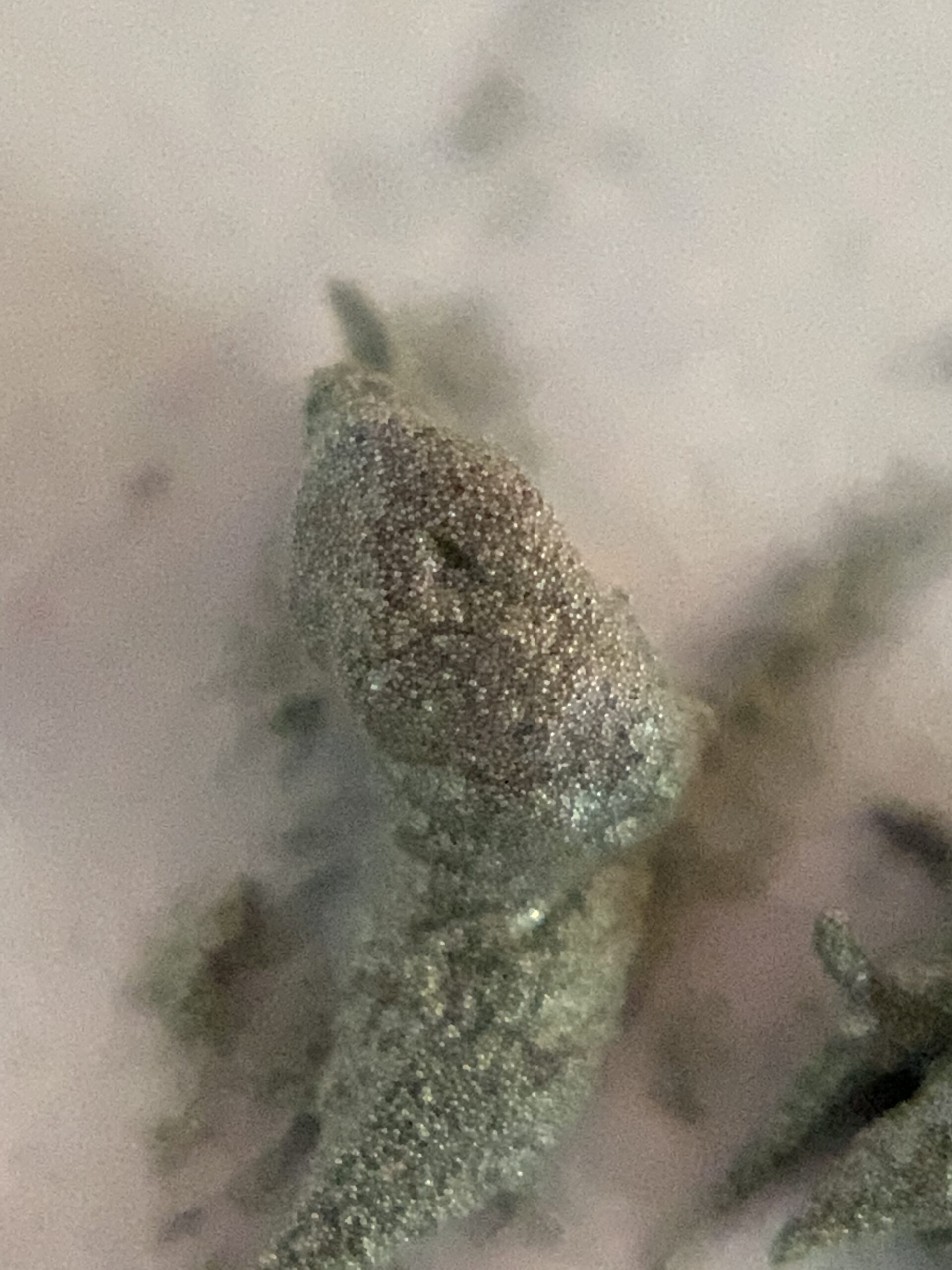
I hope you will forgive the blurriness of this second solder paste photo. The individual solder balls visible in the picture have a diameter between 0.05 mm and 0.02 mm, making it quite cumbersome to focus the camera, let alone even see them.
I carefully removed a minimal amount of solder paste from the large tub and applied it to a metal spreading tool (like the ones used for cement spreading, but much smaller). I spread the solder paste over the board, making sure I used the correct angle. The angle is critical because it will determine the amount of solder deposited. Once the solder was spread fully over the stencil apertures, I did another run with the spreader at a more obtuse angle to remove excess solder. After, I very cautiously removed the stencil, trying not to smudge the intricate planes of solder. The result was this: a beautifully pasted board!
I know I know; the paste job isn’t perfect. However, there was only one shorted trace after reflowing, so I feel that is a win!
This is, in my opinion, the most painful part of the board assembly process. Although, I do take solace in the fact that if I do it wrong, I can just wipe off the solder paste and do it again 😊.
I, unfortunately, didn’t take any pictures of the component placement process, mostly because I try to avoid leaving the solder paste sitting on the board, even though it is theoretically capable of sitting on a board for 24-hours. The small components, such as the 1 mm x 0.5 mm (0402 package) capacitors and resistors, I placed with tiny-tip tweezers. The GC-10 paste is beneficial again because of its high viscosity, which allowed me to have more confidence that the components weren’t going to move around when I transferred the board to the oven, or simply when I breathed in their general direction. I would be rich if I got a dollar for every time a 0402 capacitor went light speed when I breathed in its direction. There isn’t really much more to say about the component placement, as it is just making sure that the components are aligned on their pads and that they’re supposed to be there. I checked with a magnifying glass after placement to make sure that there were no solder paste bridges between traces, which there were none.
Now was the time for the reflow oven! I recently made the reflow oven by converting a household mini-oven. The build process also deserves its own blog post, as it was enjoyable and somewhat scary (my first ever work with AC current). For anyone curious, the reflow controller is the Controleo3 board by Whizoo. I carefully placed the board into the oven and nudged it near the temperature sensor to make sure I got the best results. I started the lead-free reflow cycle and watched in awe and anxiety. It was my first proper use of the oven; money was on the line!
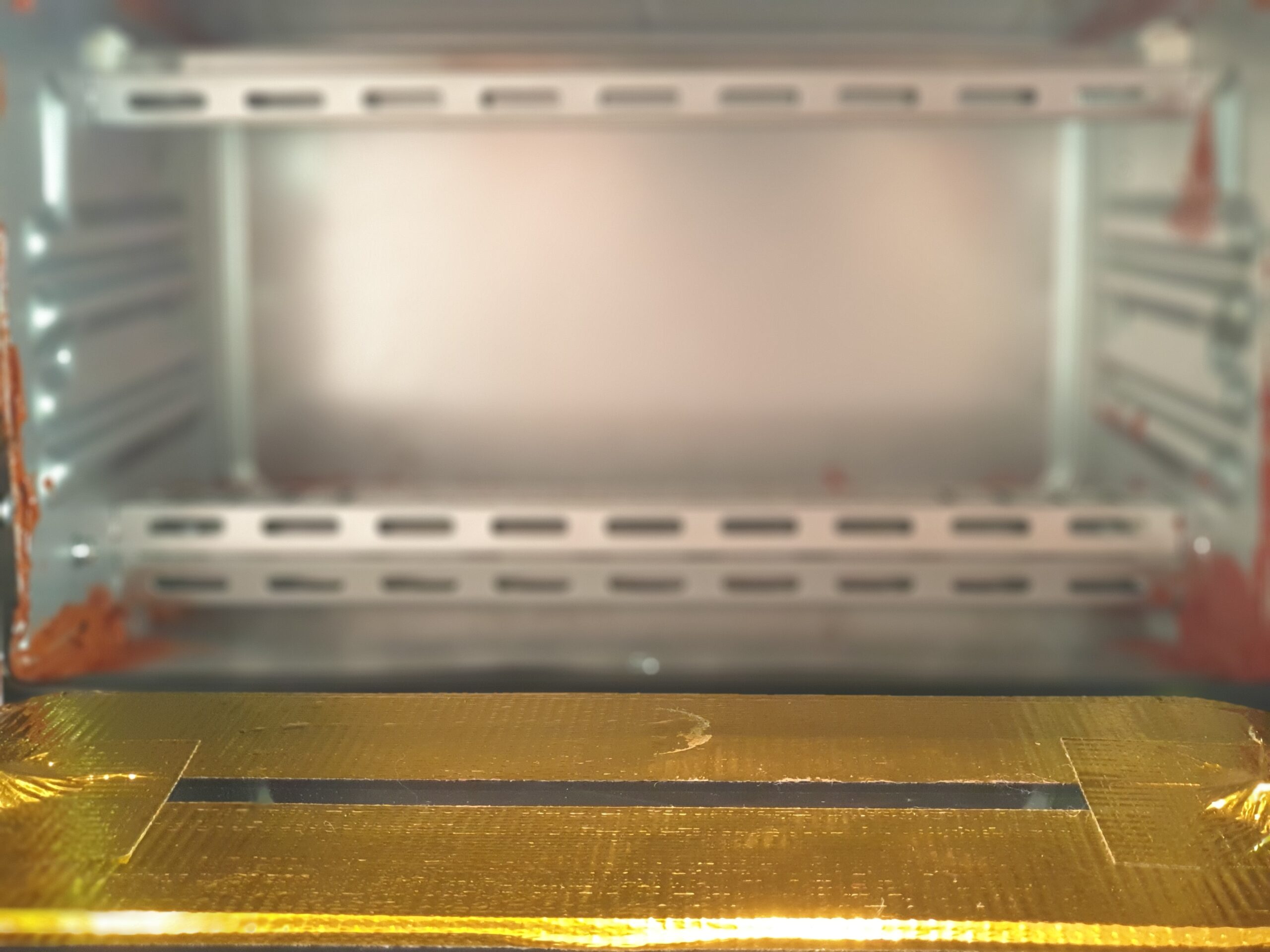
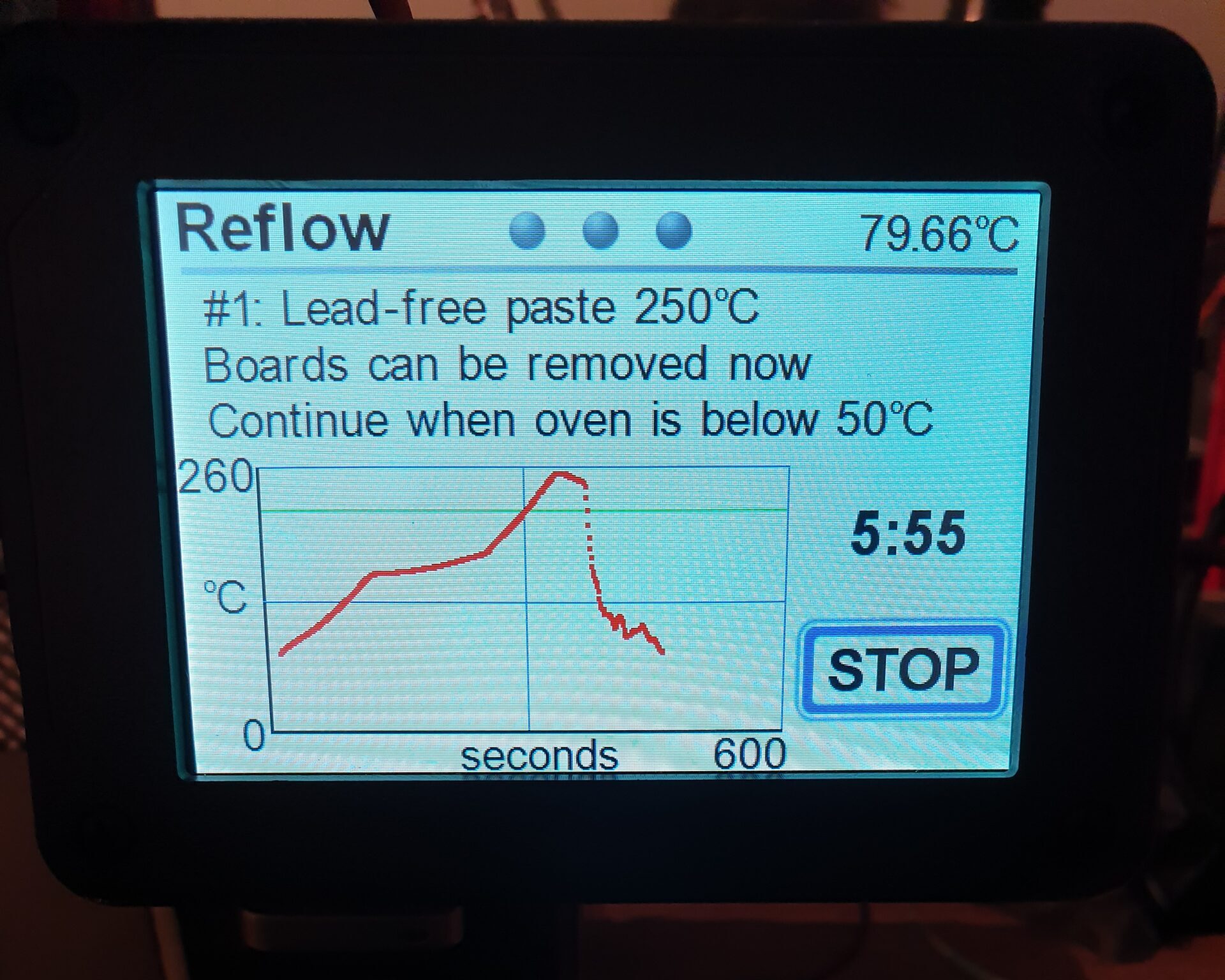
It was tough to take a picture of the board inside the oven, as there is a lack of light. Poor quality aside, you can still vaguely see the freshly baked board and the reflective aluminium cladding in the background. A barely visible golden hue is visible as well, from the gold insulation tape. Furthermore, the graph shown on the screen of the reflow controller shows the temperature during the reflow cycle. Interesting, right?
After the few minutes of anxiety-filled wait, a freshly baked board was birthed! The picture I took straight after taking the board out the oven shows how good it looked.
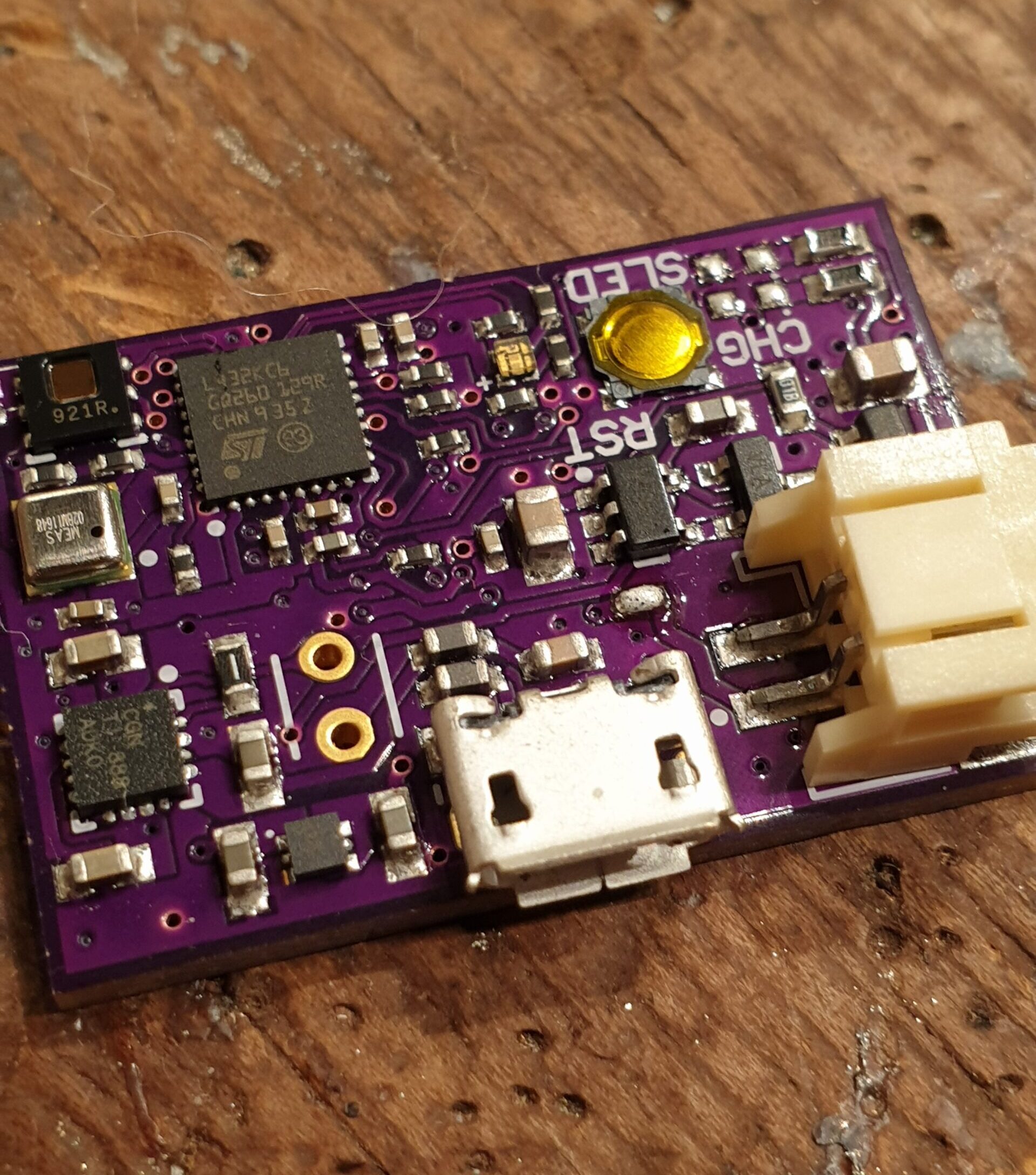
It was really super shiny, and the solder joints looked spectacular under a lens.
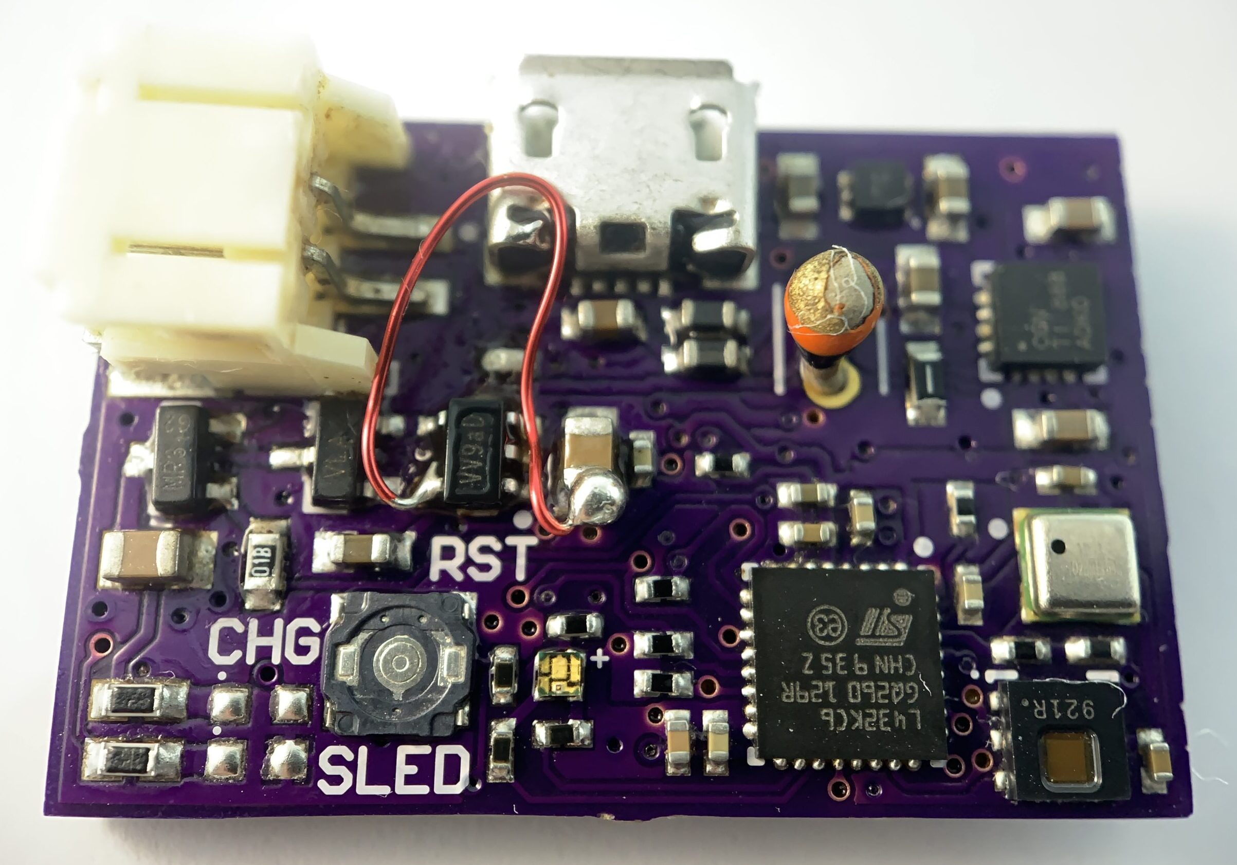
This is a picture I took recently. The board looks a bit wet because I had just cleaned it with Isopropyl Alcohol. This was done due to tiny boards like Atmospheric getting dusty unimaginably quickly. Also, don’t mind the cracked thermistor coating, I forgot why that happened.
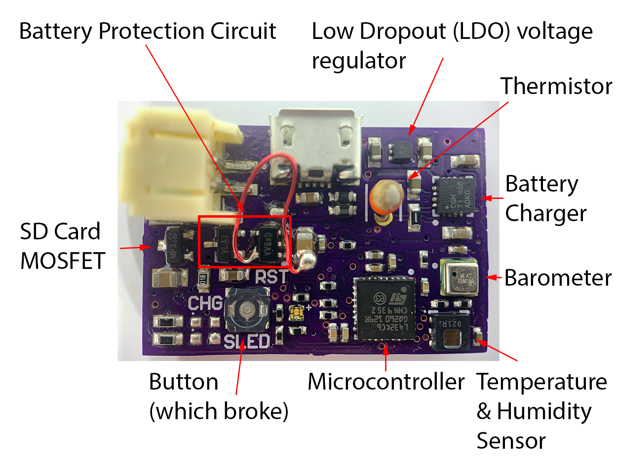
Here you can see an annotated copy of the preceding image. Not all elements have been labelled, such as the RGB LED, USB Connector, etc.
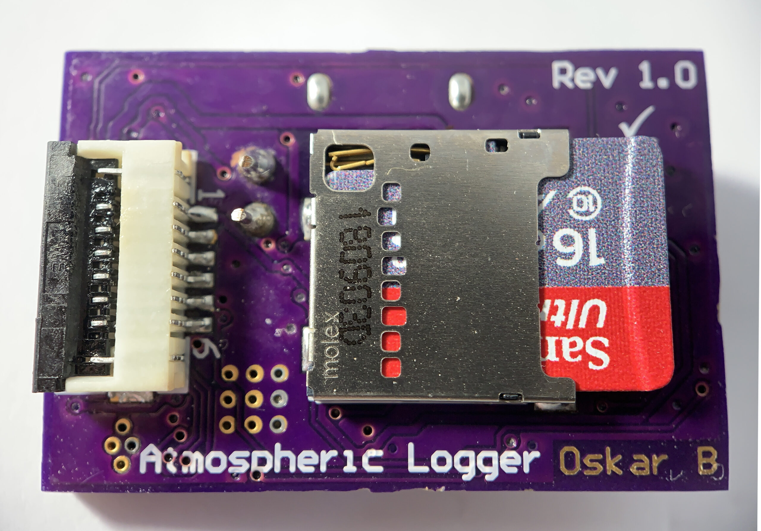
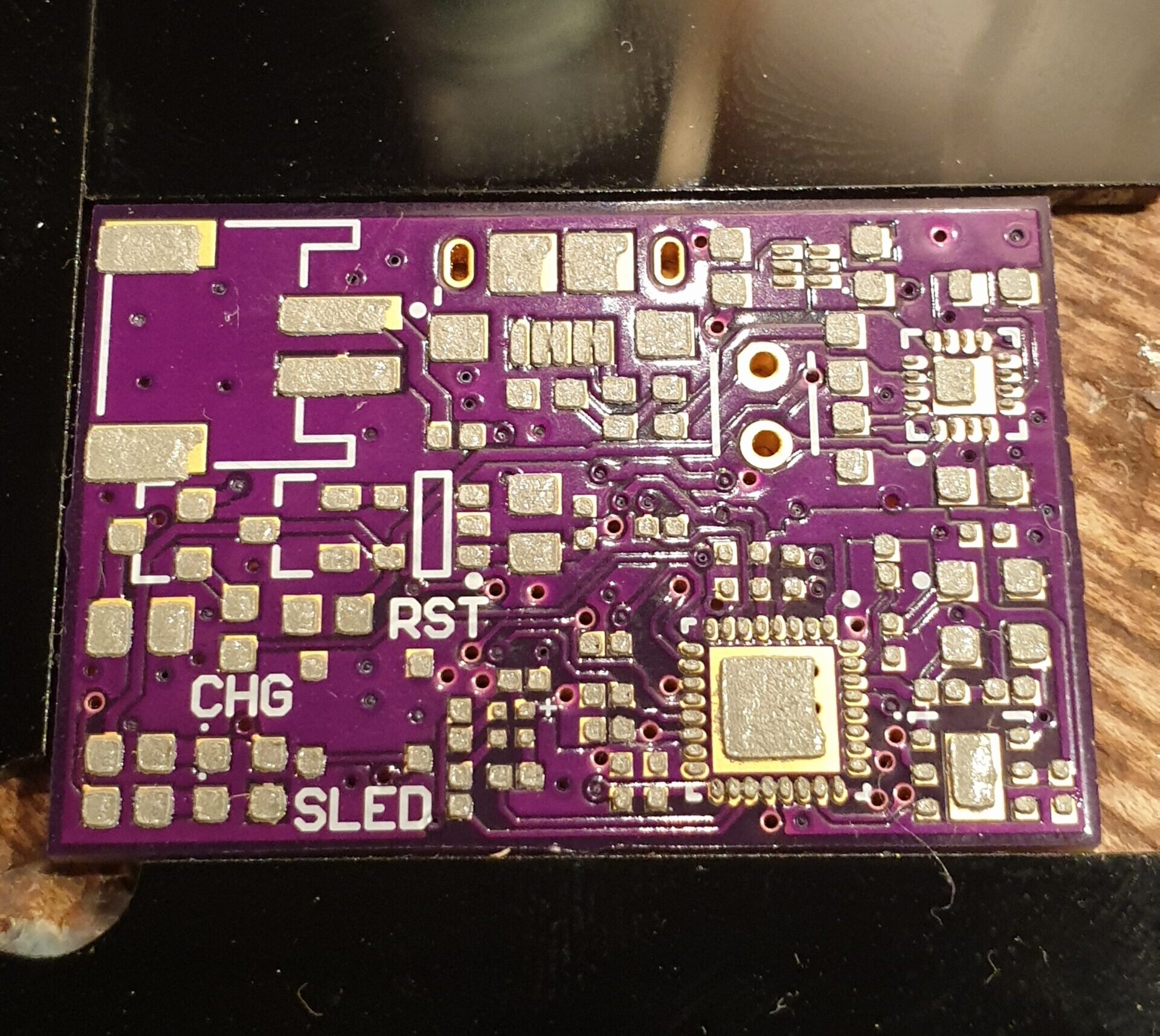
This picture shows the back of the board, with a pretty cool looking trace of my name. The tiny programming ribbon connector is visible on the left. I really should have noticed when checking the board that the “Atmospheric” text was punctured by three vias…
In the next and final part of the blog, I will go outline the physical testing of the board, programming, and issues the board faced. Lastly, I will talk about what I can improve upon in future iterations.