Hello, I hope you are doing well!
In this part of the series, I will be discussing analog-to-digital converters (ADCs) and their role in SDSense.
The Bifröst between the analog and digital world
Let’s think about the last post. To measure the current flowing through a resistor, we need to measure the voltage drop across it. Cool, but how do we do that? Maybe we could feed the output into a digital input of an Arduino. However, this is not going to tell us much because that only gives us a high or low – 1 or 0. That is 1 bit of information, which is useless if you ask me!
So, how can we get this voltage drop? This is where the very cool analog-to-digital converters (ADCs) come into play. ADCs, through a plethora of methodologies, output a binary digital signal which represents the voltage of the analog input signal. This allows for the disparate worlds of analog and digital signals to be bridged. The countless different ways ADCs can fulfil this function will not be discussed here, as it is for a whole post on its own. Sadly though, ADCs aren’t freaks of nature, and they have their limitations.
One of the major parameters of an ADC is resolution. It is somewhat analogous to a monitor’s resolution: the higher the resolution, the clearer the picture. However, ADCs measure their resolution in bits, not pixels. Remember how I said ADCs output the voltage in binary? The resolution of an ADC is the amount of these bits. An 8-bit ADC, for example, will output an 8-bit (or 1 byte!) digital value representing the analog input. You may have already spotted an issue though. Let us say this 8-bit output is at its maximum (1111 1111), which corresponds to 255. What does that mean? 255 Volts? 0.255 Volts?
Now’s where an incredibly important factor comes in, called the reference voltage. This is a precise voltage that is fed into the ADC (or internally generated). Typically, the reference voltage is the maximum voltage you can measure with an ADC, with the output representing a fraction of this value. So, let us go back to our previous example of an output from an 8-bit ADC (which we will call the output code) of 1111 1111. Now, the equation to calculate the input voltage from this is as follows:
$$ V_{in} = \text{Output Code} \cdot \text{LSB}. $$
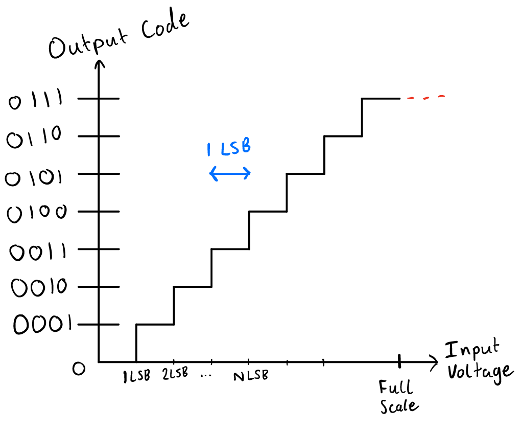
You may be wondering, what is LSB? The least significant bit (LSB) of an ADC is the change in voltage for each binary step, or simply the voltage value that a binary output of 1 corresponds too. This means that the ADC measures voltage as multiples of the LSB. The diagram below should make this much clearer.
Also, this animation I made in python shows the effect on changing the resolution of an ADC:
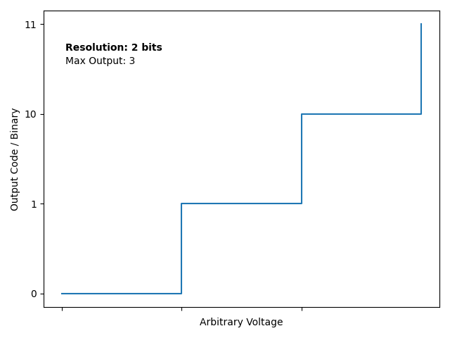
These both should show the approximating nature of ADCs. For example, input voltages of 1.4 LSB or 1.8 LSB will be shown as integer multiples of LSB – i.e. 1 LSB or 2 LSB. Here the importance of resolution should spark (hah, sorry). Now for the fun part, calculating the LSB. For a unipolar ADC (0 volts to reference voltage):
$$ LSB = \cfrac{V_{ref}}{2^N}, $$ where \(V_{ref}\) is the reference voltage, and N is the resolution in bits. The full-scale range (FSR), most typically, is calculated as:
$$ FSR = V_{ref} – 1 \thinspace \text{LSB}. $$
Nice! We are now able to calculate the LSB, FSR, and input voltage. Back again to that previous example of an output code of 1111 1111 or 255. Let us say that the voltage reference is 5 V, and it is an 8-bit ADC. What is the output voltage? $$ \begin{aligned} LSB &= \cfrac{5}{2^8}\\ &= 19.53 \thinspace \text{mV}\\ V_{in} &= 255 \cdot 19.53 \thinspace \text{mV}\\ &= 4.980 \thinspace \text{V} \end{aligned} $$
This is cool. However, there is an issue. If we think about the voltage drop of a resistor as outlined in the previous part, we know that this value is (often) in the millivolt range. Let’s say we’re trying to measure the current through a microSD card, with a 12-bit ADC with 3.3 V reference voltage. That leaves us with an LSB of \(8.056 \cdot 10^{-4} \, V\). If we use the equation \(V_{drop} = I_{load} \cdot R_{shunt},\) then we can use this minimum LSB value to determine the resistance of the shunt to get the desired 0.25 mA sensing resolution (as outlined in the prologue). $$ \begin{aligned} R_{shunt} &= \cfrac{V_{LSB}}{I_{min}}\\ R_{shunt} &= \cfrac{8.056 \cdot 10^{-4}}{0.25 \cdot 10^{-3}}\\ &= 3.22 \thinspace \Omega. \end{aligned} $$
That’s quite a high resistance for a shunt! This results in another problem – SDSense is supposed to be able to measure up to 500 mA being drawn by the microSD. If we use Ohm’s law again, with 500 mA of current through a 3.22 ohm resistor, there is a 1.61 V drop! If 3.3 V is entering the resistor, that leaves the poor microSD with only 1.69 V… That would result in a microSD card that doesn’t work.
Amplifying the fun
This is where current sense amplifiers come in! Not only do they amplify the voltage drop so that we do not need an enormous shunt resistance for our needs, but they also remove the requirement of a differential ADC. So far, I have ignored that issue. Most typically, ADCs have single-ended inputs. This means they measure their input against ground. This is a problem when we are trying to measure the difference in voltage between the input and output of the resistor, not the difference to ground! Current sense amplifiers make our lives easier by outputting a voltage that is proportional to the voltage drop between its inputs, which can be measured by single-ended ADCs in respect to ground. This output voltage is multiplied based on the gain parameter of the amplifier.
Let’s try the microSD card example again. Now we have a current sense amplifier with 20 times gain between the ADC and the resistor. The LSB will still be the same; however, the shunt resistance required will be lower.
$$ \begin{aligned} R_{shunt} &= \cfrac{V_{LSB}}{I_{min} \cdot Gain}\\ R_{shunt} &= \cfrac{8.056 \cdot 10^{-4}}{0.25 \cdot 10^{-3} \cdot 20}\\ &= 0.161 \thinspace \Omega. \end{aligned} $$Woah, that’s a lot better. Now, with 500 mA running through the resistor we will only get an 80.6 mV drop! Not incredible, but I don’t think the microSD will care. Please do note that these amplifiers aren’t a “golden gun”: they don’t perfectly amplify the voltage differential. There is gain error and other important factors, but I think it’s best to leave them out of this already lengthy post.
For both our sakes, it also would be a good idea to leave ADC and Amplifier selection to next time.
This has been a very fun post to write. I hope you enjoyed it as much as I did making it =).
Stay safe and see you soon.
p.s. please do note that I haven’t fully explained ADCs here: I have deliberately left out sampling rate, nonlinearity, and more. This is because these are better off being explained on a post dedicated to ADCs