Hello! In this post I’ll go over the schematic design for Systolic.
To help avoid this post being miles long, I’m going to constrain the scope of this post to the more important parts of the project’s schematic design. If you’d like to look at the whole schematic, please feel free to see my repo.
The isolator
We are going to take a look at the schematic design for the isolator, which includes the data and power isolating ICs.
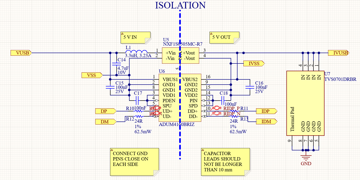
You can very clearly see I tried too hard to make this symmetrical!
Resistors R10, R11, R12, and R13 are termination resistors for the USB data lines, to help minimize signal reflection. I may go over signal reflection one day in a post, but it’s a complex topic that I don’t understand much if I’m being completely honest.
Inductor L1 and capacitor C14 are added to form an LC filter (resonant circuit), which helps the board meet conducted emission limits (for regulations such as EN 55022 and CISPR 22). This filter is outlined in the power isolator’s datasheet.
The other capacitors shown are decoupling (or bypass) capacitors, which help reduce noise on the voltage supply by acting as small “batteries”, providing current during fast current transients. Additionally shown on the right, U7, is a surge protection IC, which protects the isolated 5V rail from any high voltage transients.
Isolated Area
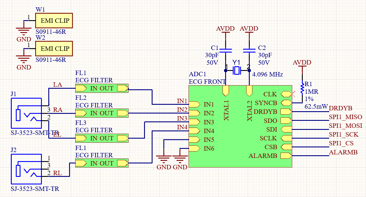
Electrode filters
The electrode filters are something that took me a very, very long time to implement (relative to the other parts of the schematic design). I wanted to make sure that I invested enough time into researching filter design so that I could trust that the filters would protect me from any hazardous events when I came to testing the ECG.
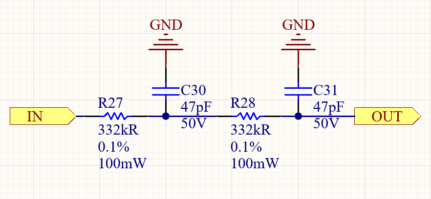
Shown here is a 2nd-order low-pass RC (resistor capacitor) filter. I simulated this filter in Texas Instrument’s TINA Spice software, with the image below showing the frequency response.
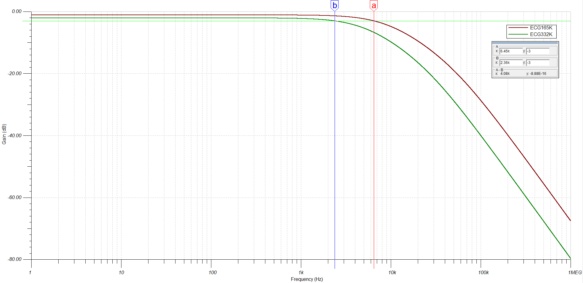
There are two curves, one showing the filter simulated with 165kΩ resistors (red), and the other 332kΩ resistors (green). The lines (b) and (a) show the -3 dB cutoff point, which is the frequency at which the filter attenuates half the power of the signal. As you can see, the red curve has a -3 dB point at 6.45 kHz, and the green curve has the point at 2.36 kHz. I won’t go into too much detail about these filters, at least not now, partly because I’m not that good with this kind of stuff!
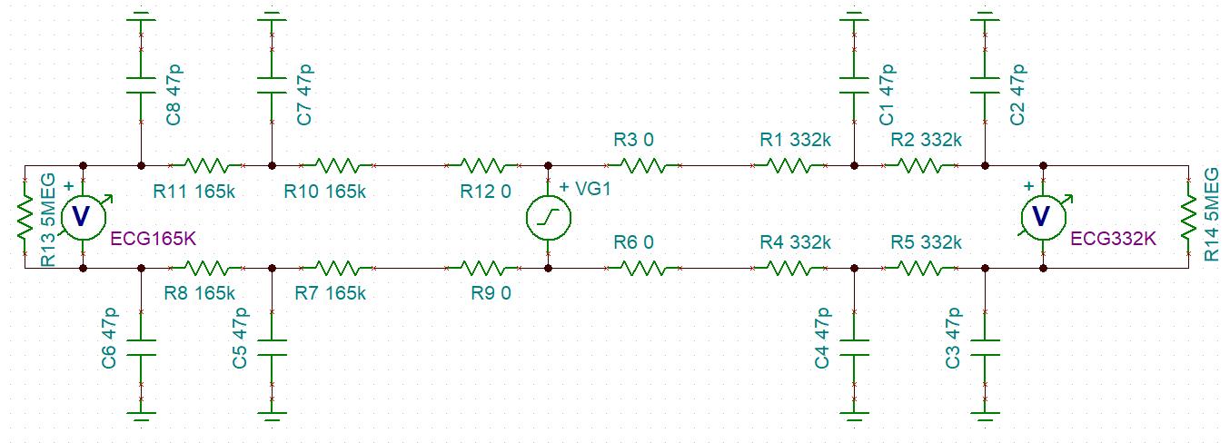
Here you can see both of the filter variations being tested, with the 165kΩ variant on the left, and the 332kΩ variant on the right.
So… Why do I need to attenuate frequencies in the first place!? The 2nd-order RC filter is low-pass, meaning it attenuates (dampens) high frequency signals and lets low frequency signals pass relatively unchanged. This is incredibly useful for the analog-front-end’s (AFE) inputs because it helps prevent high frequency noise from entering, and causing aliasing.
Aliasing is when an analog-to-digital converter (ADC) samples a signal which contains a frequency greater than the Nyquist frequency. The Nyquist frequency is derived from Nyquist’s theorem, which states (simplified) that an ADC can only sample frequencies below or at half its sampling frequency. Hence, the Nyquist frequency of an ADC is half its sampling frequency. When a frequency is present in a measured signal above the Nyquist frequency, it can “appear” as a smaller frequency, which is a big issue when in this ECG we are very interested in some of the low-frequency components of the initial signal. Thus, we need to remove these high frequencies to prevent aliasing.
Additionally, the two 332kΩ resistors act together in series as one 664kΩ resistor, which is great for protecting the user from any hazardous events on the ECG. Let's say that somehow the 5V rail managed to short to the AFE input, and the electrode is thought of as being grounded. Remembering Ohm's law that \(V = I \cdot R\), we get that \(\cfrac{V}{R} = I\). Substituting the previous values in, \(\cfrac{5 \thinspace \text{V}}{664 \cdot 10^{3} \thinspace \Omega} = 7.53 \thinspace \text{uA}\). This \(7.53 \thinspace \text{uA}\) value is good because it is below \(10 \thinspace \text{uA}\), which a critical regulatory document (IEC-60601) says is the maximum current that should be injected into a patient during a fault.We’ve implemented a filter that not only serves to prevent aliasing on the ADC input, but also protects the patient from death. Nice!
The MCU
To be honest, there isn’t too much going on with the microcontroller’s (MCU) schematic.
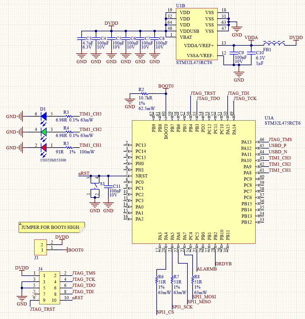
I’d like to think it’s quite neat though! In the bottom left, you can see the programming header (J4), which lets a programmer (in my case, the Segger J-Link EDU) program the MCU over a special interface called JTAG. The big block in the middle-right is the MCU itself, with its associated passive components. On the left is the RGB LED used to make debugging and use of the ECG much, much easier, and on the top are the power pins and decoupling caps for the MCU.
The AFE’s schematic is also pretty much the same as this, with no real interesting stuff going on.
One of the new ways I designed this schematic is that this schematic is hierarchical, meaning there are sub-schematic sheets, which made it possible to make the schematics clean and tidy with so many different components. This differs from the way I have designed schematics in the past, where there is just one large schematic sheet, with all the components on it. You can see what this hierarchical design looks like partially below, with each green box being an individual schematic sheet.
In the next post, I’ll go over PCB design, which was super fun for this project!
See you then.